What are the 7 different Types of logic gates?

Logic gates are electronic circuits that make logical decisions. It has one output and one or more inputs. Output signal appears only for certain combinations of input signals. Logic gates are the building blocks from which most of digital systems are built.

They implement the hardware logic function based on the logic algebra developed by George Boole, which is called Boolean algebra in his honor. A unique characteristic of Boolean algebra is that variables used in it can assume only one of the two values i.e. either 0 or 1. Hence every variable is either 0 or 1.
Gates are available today in the form of various IC families. The most popular families are transistor-transistor logic (TTL),emitter-coupled logic (ECL), metal-oxide-semiconductor (MOS), and complementary metal-oxide-semiconductor (CMOS).
Digital systems
A digital system deals with quantities or variables which have only two discrete values or states. Examples of such quantities are:
- A switch can be either opened or closed.
- A certain statement can be either true or false.
- The answer to a question can be either yes or no.
- A bulb can be either off or on.
The mathematical manipulation of these quantities can be best carried out if they are represented by binary digits 1 and o. In describing functions of the digital systems a closed switch will be represented by 1 and an open switch will be represented by 0.
Similarly, a lighted bulb will be described as 1 and an off bulb will be described as 0. We require a special algebra, known as Boolean algebra for the manipulation of the quantities which have the values 1 and 0. These values 1 and 0 are also known as Boolean variables. Boolean algebra is based on basic operations, which are (1) AND operation (2) OR operation (3) NOT operation.
Logic Voltage Levels (+ ve and –ve Logic)
To repeat the logic 1 and the logic 0 conditions in the circuits the voltage is chosen as follows +ve Logic: In +ve Logic, the 1-logic level is made more positive than the 0-logic. Usually, +5 V is assigned for logic 1 level and 0 V or ground for the 0-logic level. -ve Logic: in –ve logic 1-logic level is made more negative than the 0-logic.
Usually, -5 V is assigned for logic 1 level and 0 V for the 0-logic level. In logic circuits given below +ve logic is used. The electronics circuits which implement the various logic Operations are known as logic gates. A logic circuit has one output and one or more inputs. The output signals appear only for certain combinations for input signals. In these gates, the high and the low states i.e. 1 and 0 represent certain voltage levels. There are these fundamental logic gates are given below:
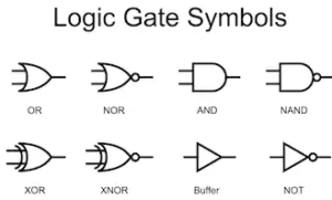
Types of logic gates
- OR gate
- AND gate
- NOT gate
- NOR gate
- NAND gate
The OR Gate
The OR gate has two inputs marked as A and B and output as C. Now A, B, and C can have one of the two states either 0 or 1. The electronic circuit for the OR gate is given below. The OR gate has output 1 and either A or B or both A & B are at logic 1.
The above circuit shows that the lamp will light up when either switch A and B or both A & B are closed. The output will be zero if and only if both the inputs or at logic zero. It means that the lamp remains off when only when both switches A and B are open. The OR gate represents the Boolean equation:

A+B = C
This equation shows that output C will be at 1 when either A and B or both A &B are at 1. The above logic operation of the OR gate can be summarized with the help of the truth table. A truth table is a table that gives the output state for all possible input combinations. The truth table for OR gate is given below Table………………..
Diode OR Gate
- When both A and B are at logic 0 i.e.connected to ground, both the diodes will be reverse biased at the output will be at zero.
- If A is at logic 0 and B is at logic 1, then Diode D1 will be reverse biased and D2 forward biased. As D2 is forward biased the output will be at logic1 i.e. at +5 V.
- If A is at logic i.e. connected to + 5 V and B is at logic 0, then D1 will be forward biased and D2 will be reverse baize. The output will be at logic 1.
- If both A and B are at logic 1, both the diodes will be forward-biased and the output will be at logic 1.
OR gate truth table
| A | B | C |
| 0 | 0 | 0 |
| 0 | 1 | 1 |
| 1 | 0 | 1 |
| 1 | 1 | 1 |
AND Gate
The AND gate has two inputs marked as A and B and output as C. Now A, B, and C can have only one of the two states either 0 or 1. The AND gate represents the Boolean equation A.B = C. From the above circuit, it is clear that AND gates give an output only when both switches A and B are closed. It means that both A & B are at 1, and the output will also be at 1. For all other combinations of the values, the A and B output is zero.

Diode AND Gate
- When both A and B are at logic 0 i.e.connected to ground, both the diodes will be forward biased at the output will be at zero.
- If A is at logic 0 and B is at logic 1, then Diode D1 will be reverse biased and D2 reverse biased. so the output will be at logic 0.
- If A is at logic 1 i.e. connected to +5 V and B is at logic 0, then D1 will be reverse-biased, and D2 will be forward biased. The output will be at logic 0.
- If both A and B are at logic 1, both the diodes will be reverse biased and the output will be at logic 0.
AND gate truth table
| A | B | C |
| 0 | 0 | 0 |
| 0 | 1 | 0 |
| 1 | 0 | 0 |
| 1 | 1 | 1 |
NOT Gate
It performs the operation of inversion or complementation. That is why it is also known as an invertor. It changes a logic level to its opposite level. i.e.it changes 1 to 0 and 0 to 1. The symbolic representation of the NOT gate. Whenever a bar is placed on any variable, it shows the value of the variable has been inverted.

For example 1 = 0 and 0 = 1 .
The bubble (o) in the symbol of the NOT gate indicates the operation of the inversion. A common-emitter transmitter whose input and the output are 180⁰ out of the phase often supplies the NOT operation. If A is at logic 0 i.e. connected to ground, the transistor is off and +Vcc appears at the output, the output is at logic 1. If A is connected to the +5 V i.e. point A is at logic 1 the transistor is on and the total +Vcc drops across R and the output is at zero, i.e.at logic 0.
NOT GATE TRUTH TABLE
| A | B |
| 0 | 1 |
| 1 | 0 |
Recent Posts
Difference between Gastritis and ulcer
Gastritis and ulcers are irritations, which must be treated urgently in order not to develop…
Saudi Arabia launches new residency plans to draw foreign talent
On Thursday, Saudi Arabia unveiled fresh residency programs geared towards drawing in skilled professionals and…
Study in UAE: Your Complete Guide to Enrolling Abroad
Studying abroad can be a life-changing experience, opening doors to new cultures, perspectives, and opportunities.…
Difference between Osmosis and dialysis
The difference between osmosis and dialysis is that Osmosis is a physical phenomenon by…
Difference between Vitamins and proteins
The Difference between Vitamins and Proteins is given here. Vitamins and proteins are essential…
Difference between Windows and Linux
The Difference between Windows and Linux is given here. Windows and Linux are operating systems…