what is the difference between p type and n type semiconductors?
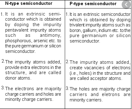
The basic difference between P-type and N-type semiconductors is that In an n-type semiconductor, there is an excess of negatively charged carriers. In a p-type semiconductor, there is an excess of positively charged carriers (holes, which can be thought of as the absence of an electron).
Difference between n-type and p-type
Depending on the type of doping material used
, extrinsic semiconductors can be further subdivided

into two classes:
- N-type semiconductors
- P-type semiconductors
N-type semiconductors
This type of semiconductor is obtained when a pentavalent material like antimony (Sb) is added to pure germanium crystal.
Each antimony atom forms covalent bonds with the surrounding four germanium atoms with the help of four of its five electrons. The fifth electron is superfluous and is loosely bound to the antimony atom. Hence, it can be easily exited from the valence band to the conduction band by the application of an electric field or an increase in its thermal energy.
Thus, practically every antimony atom introduced into the germanium lattice contributes one conduction electron without creating a positive hole. Antimony is called donor impurity and makes the pure germanium an N-type (N for the negative ) extrinsic semiconductor and with the N in a negative charge carrier.
In addition to the electrons and holes intrinsically available in germanium, the addition of antimony greatly increases the number of conduction electrons.
Hence, the concentration of electrons in the conduction band is increased and exceeds the concentration of holes in the valence band. Because of this, the Fermi level shifts upward towards the bottom of the conduction band.
In terms of energy levels, the fifth antimony electron has an energy level (called donor level) just below the conduction band. Usually, the donor level is 0.054 eV for silicon. It is seen from the above description that in an N-type semiconductor, electrons are the majority carriers while holes constitute the minority carriers.
P-type Semiconductors
This type of semiconductor is obtained when traces of a trivalent impurity like boron (B) are added to a pure germanium crystal.
In this case, the three valence electrons of boron atoms form covalent bonds with four surrounding germanium atoms, but one bond is left incomplete and gives rise to a hole.
Thus, boron which is called an acceptor impurity causes as many positive holes in a germanium crystal as there are boron atoms thereby producing a P-type (P for the positive ) extrinsic semiconductor.
As an aid to memory, the student should associate the letter P in the acceptor with the P in the “p-type ” extrinsic semiconductor and with the P in the positive charge carrier.
In this type of semiconductor, conduction is by means of holes in the valence band. Accordingly, holes form the majority carriers whereas electrons constitute minority carriers. Since the concentration of holes in the valence band is more than the concentration of electrons in the conduction band, the Fermi level shifts nearer to the valence band.
The acceptor level lies immediately above the Fermi level. Conduction is by means of movement at the top of the valence band, the acceptor level readily accepting electrons from the valence band.
For related Topics visit our page: Electronics
If you are interested in video content then watch the video:
N-type Vs P - type: