Difference between donor and acceptor impurities

An electron donor is a doping atom (impurity) that, when added to a semiconductor, can form an n-type semiconductor. An electron acceptor is a doping atom (impurity) that, when added to a semiconductor, can form a p-type semiconductor.
What is Doping?
The conductivity of an intrinsic semiconductor is not so good to use for making electronic devices. To increase the conductivity of intrinsic semiconductors, some impurities are added. This process of adding impurities to an intrinsic semiconductor is called doping. Doping is of two types:
- Accepter Doping
- Donor Doping
Accepter Doping
If the trivalent element from the III group such as aluminum (Al), boron (B), and gallium (Ga) is added to pure Si as an impurity, then the Al atom as an impurity, the Al atom occupies the position of the central Si atom in the tetrahedral structure, then one of the bonds will miss an electron. And there will be a vacancy (hole).
The numbers of holes are equal to the numbers of impurity atoms added. So plenty of free charge carriers (holes) are available for conduction. As the hole is equivalent to a positive charge, so it is called p-type material. The trivalent impurities attract electrons, so they are called acceptor impurities. After doping semiconductor is called an extrinsic semiconductor.
Majority And Minority Carriers in p-type: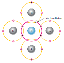
In p-type material, there is plenty of holes for conduction. So the holes are the majority carriers in p-type. There are a few numbers of electrons are present, produced by electron-hole pair production. These electrons are minority carriers are p-type. This type of doping is called accepter Doping.
Donor Doping :
The elements of V groups are pentavalent such as arsenic (As), phosphorus (P), bismuth (Bi), and antimony (Sb). These have five electrons in their valence band. When one of these materials is added to the semiconductor, four of its valence electrons form four covalent bonds and the fifth electron becomes free. The numbers of free electrons are equal to the numbers of impurity atoms added.
So plenty of free charge carriers (electrons) are available for conduction. As the electrons have a negative charge, so it is called n-type material. The pentavalent impurities give electrons, so it is referred to as donor impurities. After doping the semiconductor is called an extrinsic semiconductor.
Majority And Minority Carriers in n-type: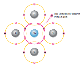
In n-type material, there is plenty of free electrons for conduction. So the electrons are the majority carriers in n-type. There are a few numbers of holes also present, produced by electron-hole pair production. These holes are minority carriers that are p-type.
Pn Junction definition: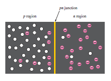
If a piece of intrinsic silicon is doped so that half is p-type and half is n-type, a PN junction forms between the two regions. The p-region has the majority of carriers holes and few minority carriers electrons. The n-region has majority carriers electrons and few minority carriers holes.
How is the Depletion Region formed in pn junction?
At the instant of the PN junction formation, the electrons near the junction in the n-region cross the junction and combine with holes in the p-region. The atoms in the n-region lose electrons and become positive ions near the junction. The atoms in the p-region accept electrons and lose the holes as the electrons and holes combine.
This creates a layer of negative ions near the junction. These two layers of positive and negative ions near the junction form the depletion region. This means that the free charge carriers are depleted from this area. Further diffusion of electrons from the n-region into the p-region forms another layer of ions on both sides of the junction. The negative ions in the p-region prevent further diffusion of electrons.
What is the Potential Barrier in pn junction diode?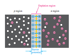
The atoms in the p-region and n-region with free charge carriers are electrically neutral. The ions across the junction produced an electric field due to which a potential difference is created called a potential barrier as it stops the diffusion of majority carriers.
If an electron has to move across the junction, it must be supplied energy equal to the height of the barrier. The typically potential barrier is approximately 0.7 volts for silicon and 0.3 volts for germanium.
Energy Diagrams of PN junction and Depletion Region:
Due to differences in the atomic characteristics of the pentavalent and trivalent impurity atoms, the valence and conduction bands in an n-type material are at slightly lower energy levels than the valence and conduction bands in a p-type material.
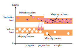
The free electrons from the n-region can easily diffuse across the junction into the conduction band of the p-region. They then lose energy and fall into holes in the p-region valence band. As the diffusion continuous, the depletion regions begin to form, and the energy levels of the n-region decrease. This is due to the diffusion of higher-energy electrons to the p-region. When the overlapping to bands is misaligned, the diffusion stopped and the junction is at equilibrium.
Watch also:
For related Topics visit our page: Electronics
One Comment